Active 6 years 6 months ago. The dut is instantiated into the test bench and always and initial blocks apply the stimulus to the inputs to the design.

Silos Supports Verilog Hdl Ieee 1364
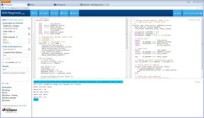
To design all logic gates in verilog and verify.

Test bench in verilog for and gate. If neither input is high a low output 0 results. Vhdl code for and gate using modelsim how to use modelsim duration. This video helps you to create test bench in verilog more on test bench.
You can modify the test bench with vhdl verilog programming in the test bench generated. 2 a verilog hdl test bench primer generated in this module. Testbench is another verilog code that creates a circuit involving the circuit to be tested.
I have written a simple test bench for and gate. A high output 1 results if one or both the inputs to the gate are high 1. A structural approach consist in designing all components needed for the design such as gates to form subsystems and then joining them together to form a larger design like adders and arithmetic logic unitsetc.
Vhdl or gate code test in circuit and test bench this video is part of a series which final design is a controlled datapath using a structural approach. This video will provide the easiest way to generate a test bench with altera modelsim. Connect with me here archive.
Follow intel fpga. In such cases testbenches are very useful. Also the tested designs are more reliable and prefer by the clients as well.
Suppose input is of 10 bit and we want to test all the possible values of input ie. Verilog code for and gate with test bench. Test bench for writing verilog output to a text file.
Verilog test bench code. Next we will write a testbench to test the gate that we have created. Sujeet singh 47050 views.
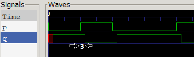
While loop in test bench of and gate. 210 1 then it is impossible to do it manually. The or gate is a digital logic gate that implements logical disjunction it behaves according to the truth table to the right.
Ask question asked 6 years 6 months ago. The outputs of the design are printed to the screen and can be captured in a waveform viewer as the simulation runs to monitor the results. If the output becomes to the input of the one gate then the code for the gatehow the code look like.
This code will send different inputs to the code under test and get the output and displays to check the accuracy.

Full Adder In Verilog
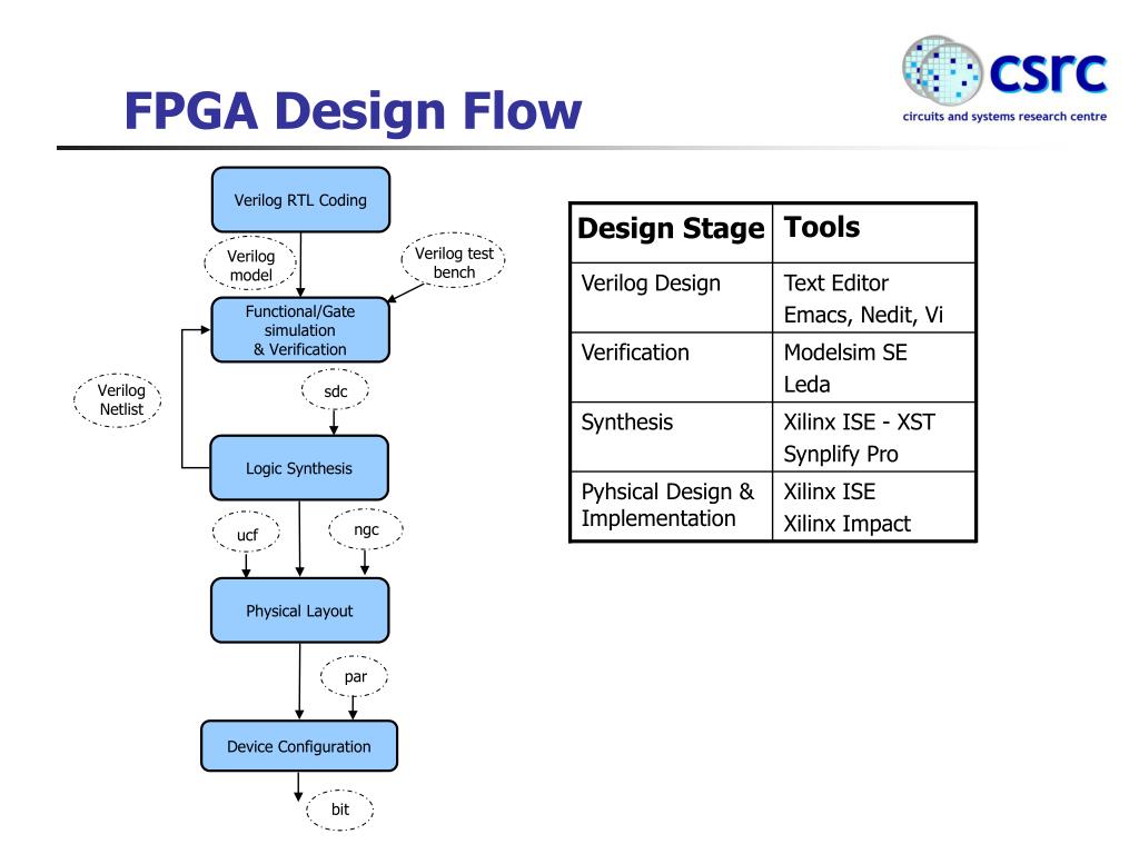
Ppt Fpga Design Flow Powerpoint Presentation Free Download Id
And Or Not Xor Nand Nor Verilog Code Electronics Hub

National Taiwan University Verilog Hdl Overview Prof An Yeu Wu
Gate Level Modeling Part Iii
Ic Applications And Hdl Simulation Lab Notes Hdl Code To Realize
Vhdl And Verilog Test Bench Synthesis
Learning Verilog For Fpgas The Tools And Building An Adder Hackaday
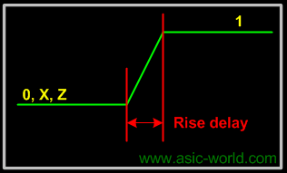
Delay In Verilog
No comments:
Post a Comment